

Printed circuit boards (PCBs) are the backbone of modern electronics, allowing for complex and powerful circuits to be housed in ever smaller packages. By stacking layers of circuits on top of one another, multilayer PCBs manage to pack billions of connections into very small spaces, and today they’re found everywhere, from our watches and phones, to our cars, and even to our household appliances. And they’re printed on every kind of material, including cloths and plastics.
But while PCBs have been around for decades, important new discoveries and advances are still being made all the time, and one of the most exciting recent advances involves high-intensity Pulsed Light.
In a nutshell, Pulsed Light provides a faster and more reliable approach to curing the metallic circuitry that makes up the nervous system of any PCB, speeding up production while improving quality. And now, those advantages can be applied even to multilayer PCBs.
Building on success
Using Pulsed Light for PCB sintering is not new in itself. Research reports–-like this one on nature.com–-have demonstrated that Pulsed Light can sinter conductive materials like copper and silver with greater speed and precision than other methods, making it ideal for creating more reliable and robust printed circuits. The technology is well established in the printed electronics industry, where circuits are printed on flexible surfaces using metallic inks and then cured with Pulsed Light.
But multilayer PCBs have always posed a challenge because some layers of circuitry are, by definition, “hidden” behind other layers. If the energy of the Pulsed Light doesn’t reach all the circuitry in sufficient doses, the metals won’t cure properly.
The question was, could we find a way to bring the advantages of Pulsed Light to multilayer PCBs, as well as to other more complex applications? If so, it could have a big impact on the industry.
Teaming up with our partners
We started with the XENON X-1100, the advanced, highly-integrated laboratory R&D system that scientists, engineers and researchers use to experiment and define processes for new applications. This system has been proven for some time in the printed electronics industry.
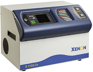 Then, working closely with our partners, we developed the XENON X-1100/2x, a more powerful version of the same system to expand its capabilities and potential applications. Where the X-1100 is able to produce 3.8 Joules of energy per square cm, the X-1100/2x can produce twice that amount—up to 7.5 Joules per square cm. Yet it’s still contained in a benchtop unit designed and priced for the R&D lab, available as a stand-alone system or as a field upgrade for existing X-1100 customers.
For the first time, research engineers and scientists can explore higher energy Pulsed Light applications without having to invest in larger and more expensive systems. The X-1100/2x puts new cutting-edge research on the table, quite literally, including its potential use in multilayer circuitry and other applications that previously were not practical.
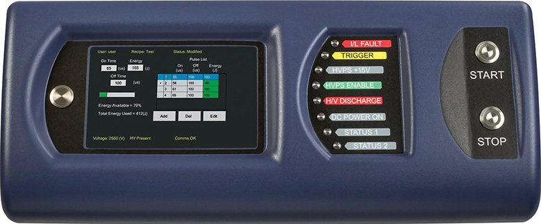
A user-friendly touch screen interface makes it easy to customize pulse parameters such as energy, duration, and timing. The system can calculate the energy from the voltage and pulse width set by the user and also measure the actual pulse using a built-in oscilloscope.
Looking ahead
Research using the XENON X-1100/2x is already underway, as companies are exploring new ways to apply Pulsed Light to improve production speed and quality. Since PCBs are used everywhere, there are many possible applications in everything from wearable technology and consumer electronics, to medical devices and aerospace.
Of course, Pulsed Light’s effectiveness depends on many factors such as the number of layers, substrate material, types of inks and metals, and so on. This is why it’s important to have a practical yet powerful benchtop R&D system like the X-1100/2x, so that researchers can discover the optimum combination of materials and processes.
If you would like to work with XENON to develop new solutions powered by XENON Pure Pulse Technology™, we’d like to hear from you. Contact XENON Corporation today to discover how our sintering technology can elevate your products and research to the next level.